The two stages behind every electronic device
Every electronic product — a drone, a robot, a phone, a smart device — starts as a bare printed circuit board and becomes a working assembly through surface-mount technology. In Shenzhen, both stages happen at enormous scale, often within a few kilometers of each other. Understanding them on a factory floor is very different from reading about them online.
Stage one: PCB fabrication
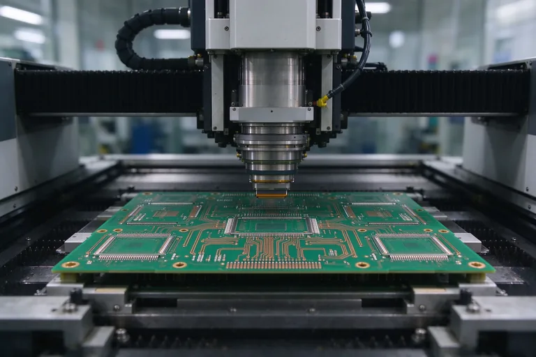
PCB fabrication is the process of manufacturing the bare board itself. On a visit, you can typically see or learn about:
- Inner layer processing — copper layers coated, exposed and etched to form the conductive traces in multilayer boards.
- Lamination — layers pressed together under heat and pressure.
- Drilling — precision machines drilling the holes that connect layers and accept through-hole components.
- Plating — copper deposited electrolessly and electrolytically to create connections through the holes.
- Outer layer etching, solder mask and surface finish — the green (or other color) protective layer and finishes such as HASL or ENIG.
- Routing and testing — boards cut to final shape and electrically tested for continuity and shorts.
Fabrication is capital-intensive and highly automated. Seeing the precision equipment explains why board quality and manufacturing capability vary between suppliers.
Stage two: SMT assembly
Once a bare board exists, components are mounted onto it. Surface-mount assembly is one of the most visually striking processes in electronics manufacturing:
- Solder paste printing — paste applied through a stencil onto the pads where components will sit.
- Solder paste inspection — automated checks that the right amount of paste was deposited.
- Pick-and-place — high-speed machines placing hundreds or thousands of tiny components, including microchips, resistors and capacitors, with precise positioning.
- Reflow soldering — boards pass through controlled ovens that melt the paste and form reliable joints.
- Automated optical inspection (AOI) — cameras and software checking for missing, misaligned or poorly soldered parts.
- Functional and in-circuit testing — completed boards tested against the design requirements.
Through-hole parts, final box assembly and packaging often follow in separate areas.
What hardware teams should look for on a visit
If you are evaluating a manufacturer rather than simply observing, pay attention to a few practical indicators:
- Inspection and testing capability — AOI, testing equipment and documented quality processes.
- Prototyping and small-batch support — whether the factory handles early-stage runs before mass production.
- Lead times and flexibility — typical turnaround for boards and assemblies, and how changes are handled.
- Certifications and documentation — quality standards and the records available for your product.
- Communication — how engineering questions, design files and revisions are managed.
Why Shenzhen's ecosystem matters
A single factory rarely does everything. What makes Shenzhen unusual is the density of the full chain — board fabrication, component markets, SMT assembly, injection molding, 3D printing and final assembly within a short distance, alongside the Huaqiangbei markets where many products begin as a handful of sourced parts. Walking through even part of this chain makes the speed and flexibility of Shenzhen manufacturing concrete.
Arranging a PCB or SMT visit
Production floors require advance arrangement and a business introduction — they are not open to walk-in visitors. TechVoyage organizes visits to PCB and SMT facilities as part of factory and manufacturing programs, combined with Huaqiangbei, 3D printing and, where relevant, robotics company visits. Tell us your goals and dates and we'll explain what we can arrange.
See the manufacturing chain firsthand
Message us to plan a PCB and SMT factory visit.
Arrange on WhatsApp
 Tech
Tech